Podcast: Play in new window | Download
Subscribe: Apple Podcasts | RSS

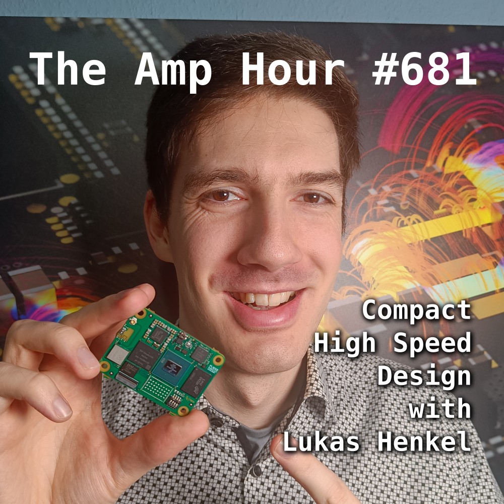
Welcome Lukas Henkel of OV Tech GmbH, a product design firm based in Nuremburg Germany!
- Miniturization and the limits of miniturization
- Price is a constraint
- Using standard PCB tech (off the shelf)
- Open source SIP
- Steps
- Conventional pcbs / components
- Silicon inductors embedded in boards
- Bonded Bare dies / stacked
- Need volume to make it work
- Requirements to fit into ______
- iMX8 ULP – 0.4mm CSP
- SIP Footprint
- Module abstraction layer talk
- Framework laptop
- Software support / BSP
- SIP will be different than PiMX8
- Crowdsupply campaign launching 2-3 weeks and delivery in Dec/Jan
- OpenSource laptop
- CM4 vs PiMX8
- SPI Flash with backup partition
- Secure element SE050
- Footprint for coral tpu and Halo 8
- Trying to solve the problem of vision use cases
- Marketing using layout / products but also making money on it
- Katerina show
- Visualizing simulations
- Developing intuition
- OpenEMS
- Usability is based on python scripting
- Using Blender for heat map
- BVTKNodes uses .vtk file output
- Multiphysics solvers
- Things that drive Lukas
- For HDI, Thinking in 3D / 2.5D and being able to visualize
- Layers ranging from 4 to 18
- Any layer design for SIP
- Wurth electroncis for high density “any layer stackup”
- Article series on altium for the open laptop
- Follow Lukas on LinkedIn
Lukas also was a co-founder of PCB Arts. We had his cofounder Saber on the show in the past.

Great show. Lukas work is great. What is “the consultants forum”? – Thx!
The consultant forum is a quasi private section for consultants on the Contextual Electronics forum. Apply here: https://docs.google.com/forms/d/e/1FAIpQLScYmuF7i3FyxY1j5sR72OSXqLI3j4UUAzIMsIL6Vn49HTXDYQ/viewform